Transmission Lines in Digital Systems
More exciting than it sounds!
Table of Contents
The Theory (And Proving it Works)
All of us with a typical electrical engineering degree learned basic transmission line theory in school. Stuff about signal reflections, propagation delay, electrical length, etc. A big take-away we learned is that the optimal case for transmission is when ZSOURCE = Z0 = ZLOAD. Ok, sounds fine.
What about digital systems though? In common digital systems your transmitting side will be some push-pull CMOS output or similar, so its source impedance is nearly zero - way less than 50 ohms. And your receiving side is some high impedance CMOS input - a load impedance way greater than 50 ohms. But for signal integrity, we're told that the transmission line between them (the trace on your PCB) should be routed as 50 ohms.
But where does this "rule-of-thumb" come from? Why should it help when neither the source nor the load impedances are close to 50 ohms? Well let's dispell the myth. I'm here to tell you that in a digital system, just routing your traces as 50 ohms won't save your signal integrity on its own. The advanced-rule-of-thumb solution, of course, is to add a termination - usually 50 ohms.
Terminations - Why Should They Work?
But hang on a minute - didn't we agree above that the source impedance needs to match the load in order for this to work? Otherwise you'll have reflections - and hence - bad signal integrity ... right? Well, not quite. High speed digital design is an exercise in freeing your mind. Reflections aren't necessarily the enemy, as you'll see shortly. I'll talk more theory as we go, but let's get into the fun stuff now.
Test Setup
It turns out that my Siglent SDG2042X function generator has a 50 ohm termination in its output path at all times, which messes up what I'm trying to show. Its rise time also maxes out at ~8ns. So first I constructed a 74-series logic buffer by connecting six SN74HC14 inverters in parallel. I wanted to ensure I had enough drive strength so the rise and fall times would be as sharp as possible. My scope measured the rise time at just under 3ns with a 3.3V supply. Good enough.
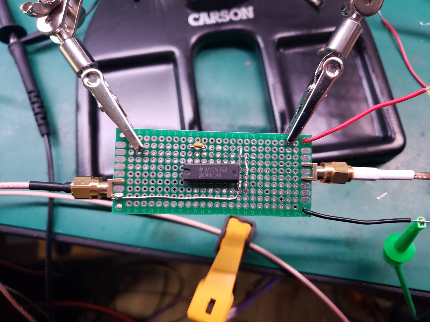
A SN74HC14N soldered to a perfboard. Signal in on the right, signal out on the left (sorry it's backwards).
Baselines
With nothing connected, just scoping the output (Rigol DHO4804, 500MHz x10 passive probe), I got the below result. Lots of over/under shoot, huh? Amazing what just a short length of wire can do to a signal.
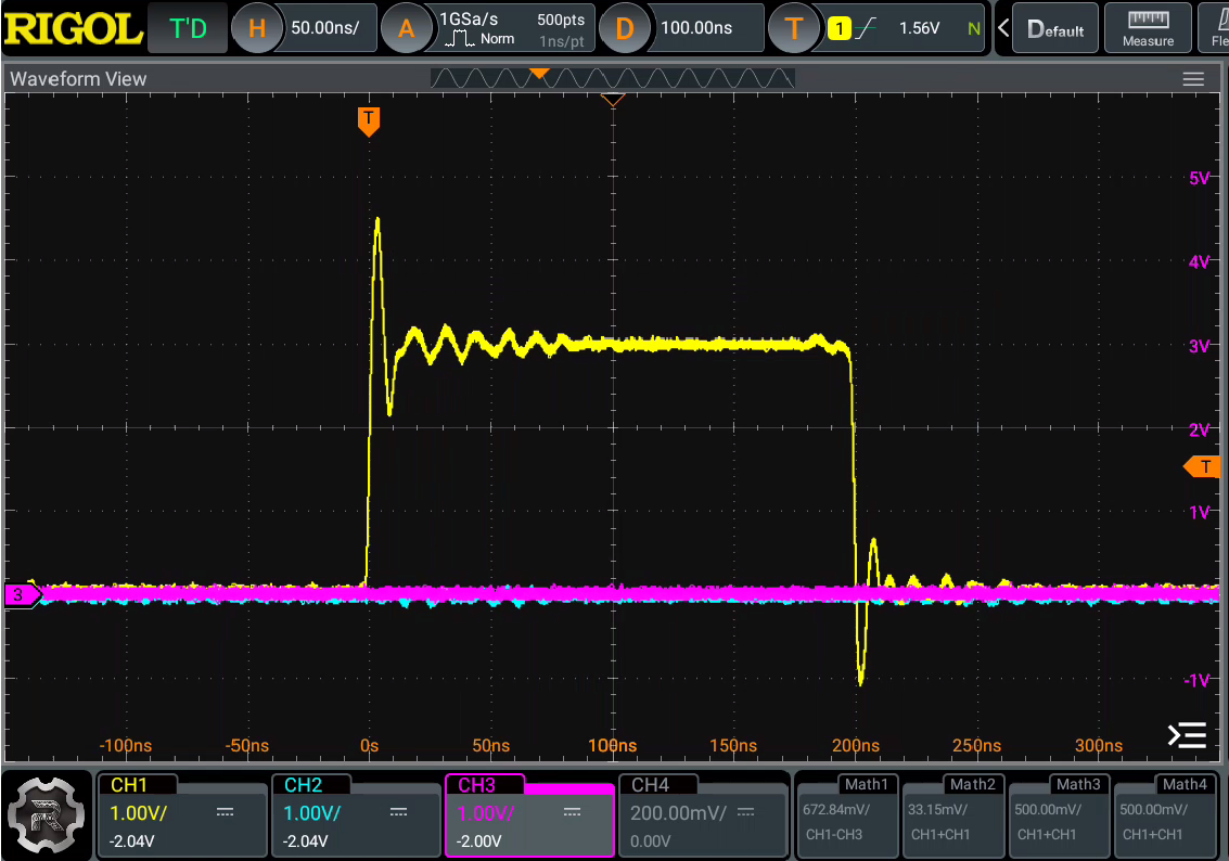
Baseline output
Unterminated Transmission Line
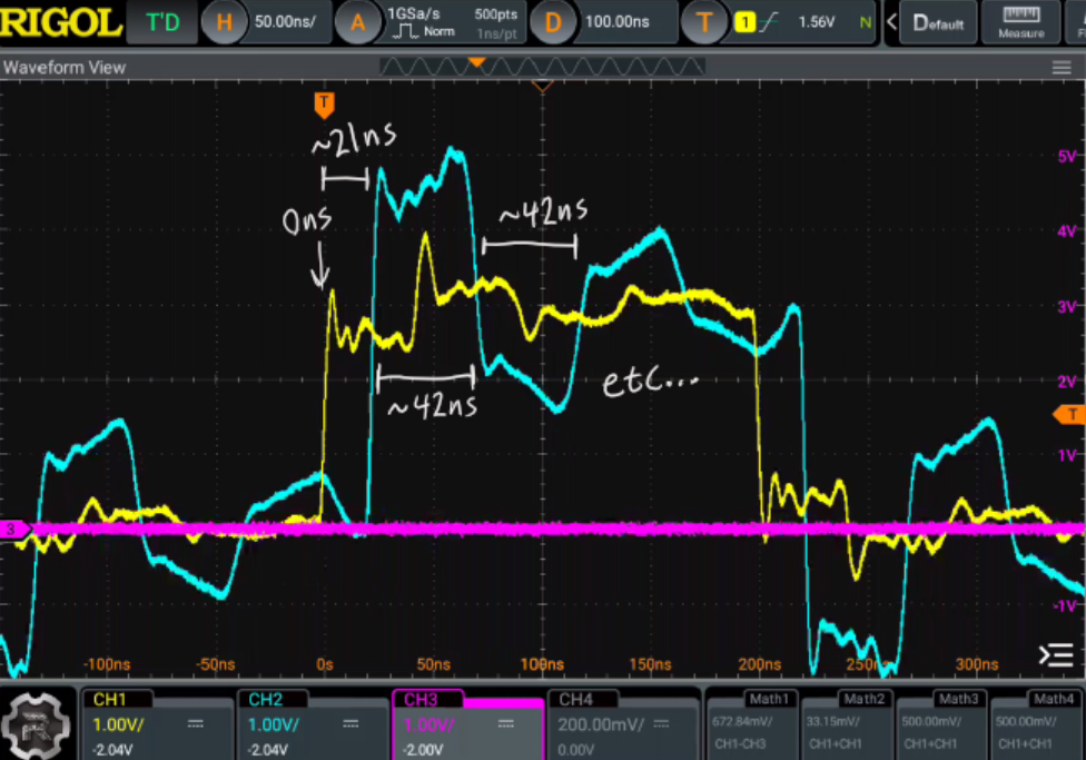
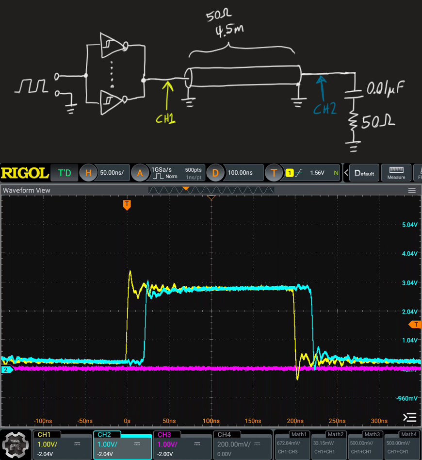
I gathered up all the SMA cables and F-F adapters I had on hand and fashioned a long (4.45m) 50 ohm transmission line. I hooked this up to my buffer and scoped the start and end of the line. Take a look:
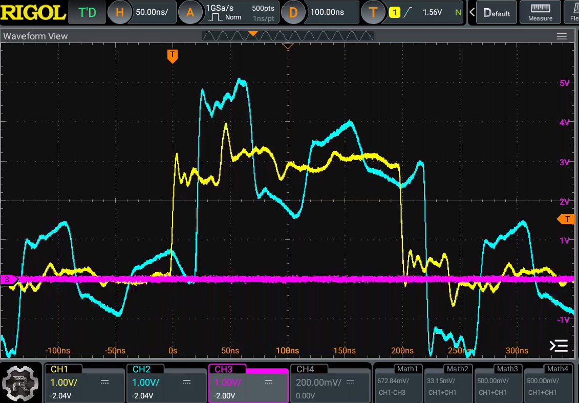
About as bad as it gets. CH1 (yellow) is start of line, CH2 (blue) is end of line.
What you're seeing there are the reflections from the energy bouncing back and forth from start to end. Increasing the period of the square wave, we can see that eventually the reflections die down as the energy is dissipated in the resistance of the line.
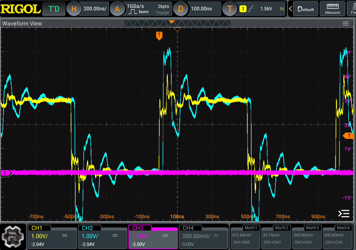
Reflections dying down with longer square wave period.
Let's take a moment to make sense of what we're seeing. First let's figure out what we should expect for the time this signal will need to propagate down the line. Cue the napkin math:
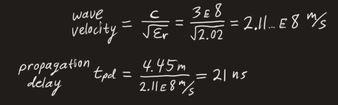
Calculating propagation delay.
Breaking down the reflections.
Simple End Termination - Why Does it Work?
End termination is easy to buy into and believe it should work (and indeed it does work):
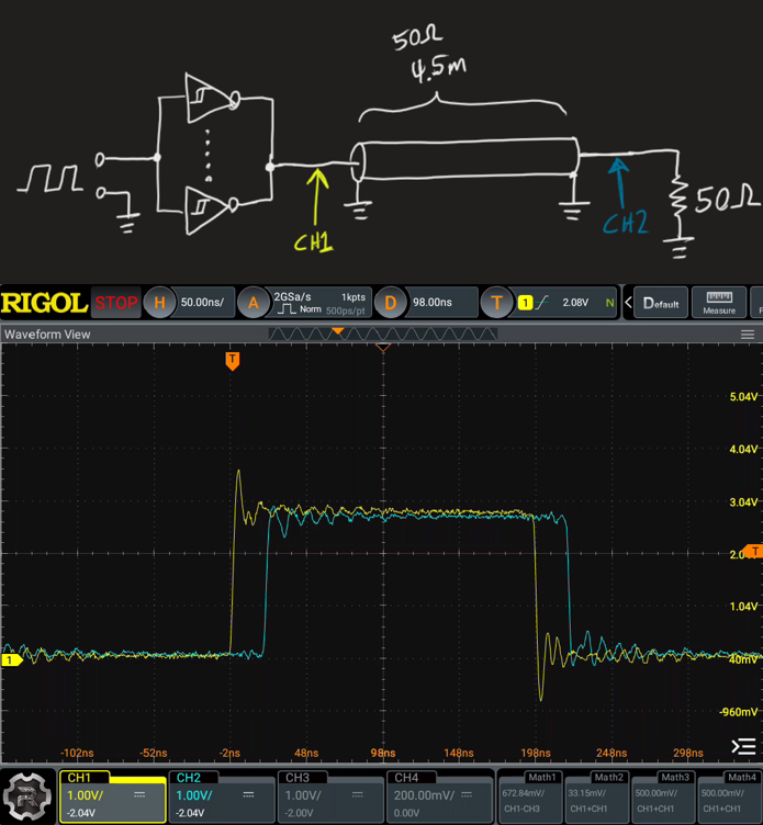
Schematic of setup and scope waveform.
But let's think deeper for a moment. WHY does it work, when the source impedance is still not matched to the load whatsoever? I think about it in terms of energy transfer. Remember that the transmission line is primarily distributed L's and C's, thus it's primarily reactive (resistance is there too, but small enough for now to forget about). But looking into a very long (read: infinite) transmission line, the line will in fact look resistive to whatever is driving it. Our transmission line is not infinite, but on the timescale of nanoseconds, it might as well be. So when the buffer starts driving the line, it has the task of charging and magnetizing the distributed C and L. The energy is the time-integral of V
This feels like a roundabout way of describing all this, but typical explanations of end terminated digital systems use math to prove the point, whereas I wanted to have an intuitive understanding of what's going on. Hopefully this gives you some additional perspective too.
Source Termination
A simple end-termination is often undesireable for some perhaps-obvious reasons. For one thing, with a 3.3V signal for example, the average current through the 50 ohm resistor is ~33mA, not to mention that while the output is high, the current required will be ~66mA during that time!
Another way to terminate this system is a source termination. Simply placing a 50 Ohm resistor between the logic gate output and the transmission line. Take a look at what happens:
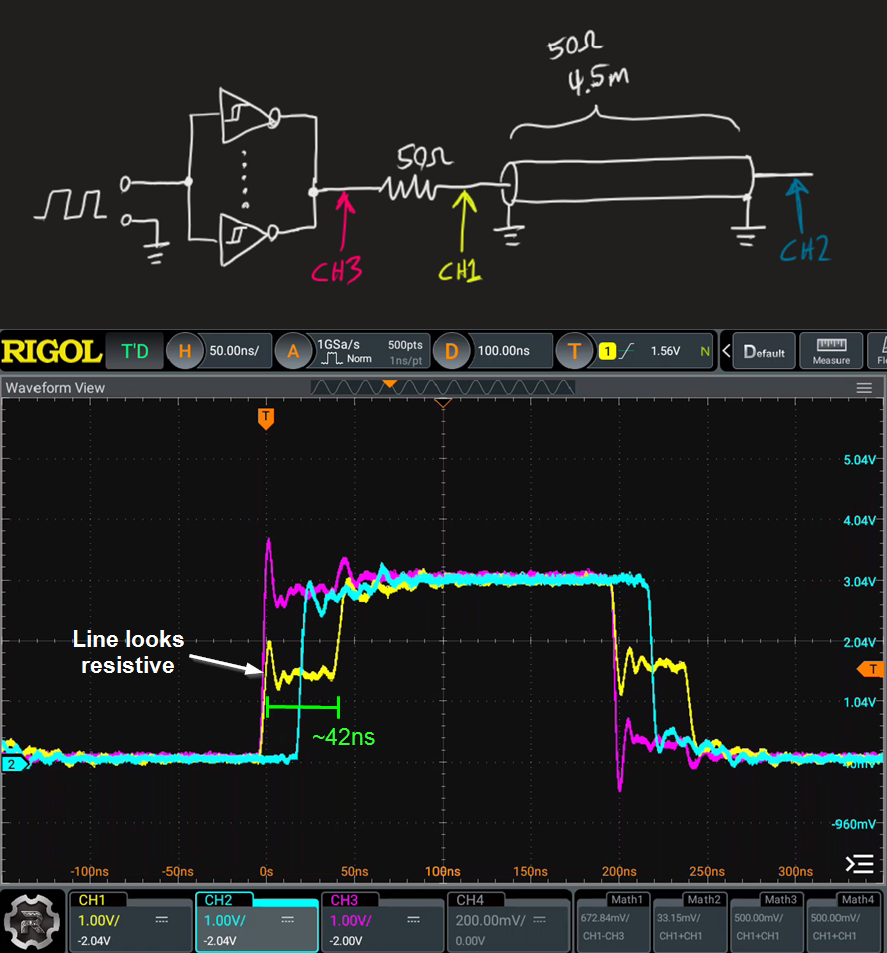
Schematic of setup and scope waveform.
Let's unpack what's happening. Initially, the transmission line looks like a 50 Ohm resistive load, so we see the amplitude of the pulse cut in half at first. We are delivering a 50 ohm signal into a 50 ohm transmission line. The energy propagates down the line, and after 21ns it hits the end of the line and sees a near-open-circuit (10M ohms of our scope probe), thus the energy is reflected back completely. A complete reflection at an open circuit means the voltage amplitude will show up as twice the incident amplitude (a mountain comes back as a mountain). After another 21ns, the reflected energy reaches the start of the line, and the 50 ohm signal is completely absorbed by the series 50 ohm resistor, causing the voltage to add at that point to equal the full pulse amplitude.
I like this experiment because it shows us very visually how characteristic impedance works. The impedance of the line is primarily reactive - no power is dissipated in the distributed L and C of the line. So whatever energy is delivered into the line will need to be dissipated somewhere, else it will reflect off the ends and bounce around for awhile until the small parasitic resistances in the system cause it to die down. But while the impedance is reactive, it appears to an incident wave as resistive. Only when the wave bounces back and is absorbed by the source termination does the line reach an equllilbrium.
RC Termination
What if you only have access to the end and can't change the source, so you're stuck with end termination? But say you don't want all that DC current draw and dissipation that comes with slapping a 50 ohm resistor at the end of the line. Enter the RC termination. It's basically just like a simple end termination, but with a cap in series, so you don't have a DC component falling across the 50 ohm resistor.
Schematic of RC termination circuit and waveform result.
Current Draw Calculation
Briefly I want to show how to roughly calculate what DC current you can theoretically expect for each of these situations. Then I'll show actual data I took on how much DC current each circuit draws. Because nobody is ever really convinced by just math, right?
In my experimental setup, I powered the buffer from a 3.3V bench supply routed through my HP 34401A manually set to the 100mA range. I fed in a 2.5MHz 50% duty-cycle square wave, and recorded the numbers. But first let's predict what we should see in an ideal world.
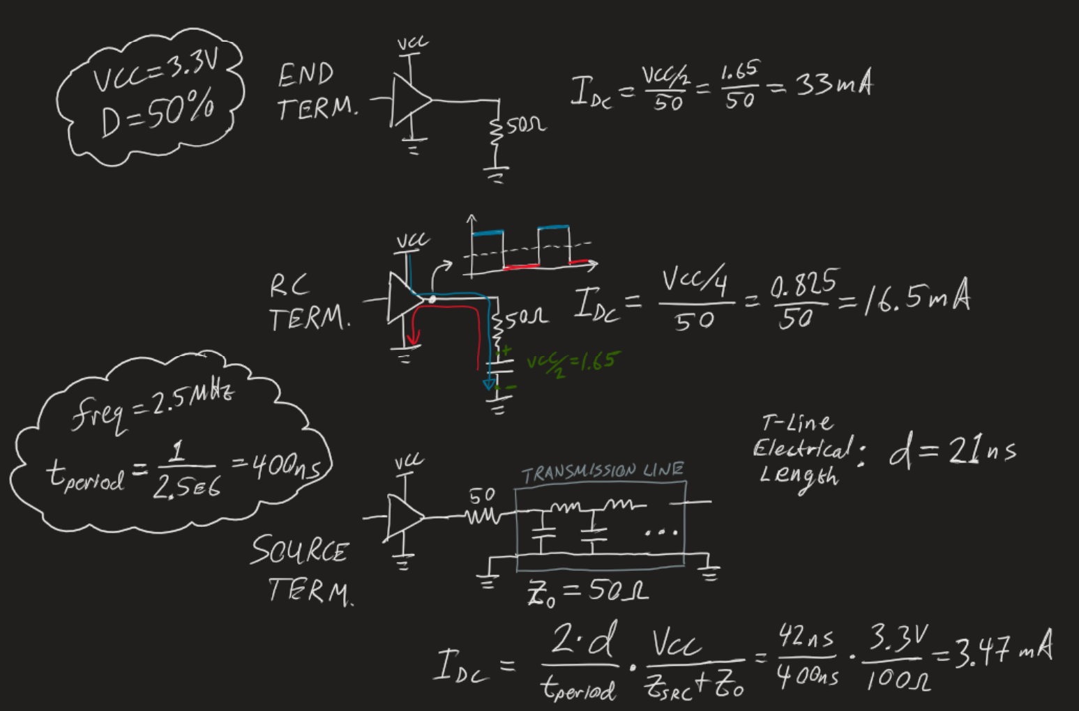
Calculations of current draw for different termination strategies.
Current Draw Empirical Results
| Circuit | Ideal (Calc'd) Current Draw | Measured Current Draw |
|---|---|---|
| 50 Ohm End Term. | 33mA | 25.7mA |
| RC End Term. | 16.5mA | 14.4mA |
| Source Term. | 3.47mA | 4.25mA |
| Open (No Term.) | ???mA | 3.57mA (!!) |
Source terminated looks like a good deal, right? You may be tempted to think that this results in the lowest drive-strength requirement for our logic gate, but not so. Doing an LTSpice simulation lets us peek at the current more closely. You can see that while the average current is ~3.47mA (as the prophecies foretold), the current the buffer has to deliver while the wave is propagating down the line is indeed 33mA, as though the buffer is driving a 100 Ohm resistive load.
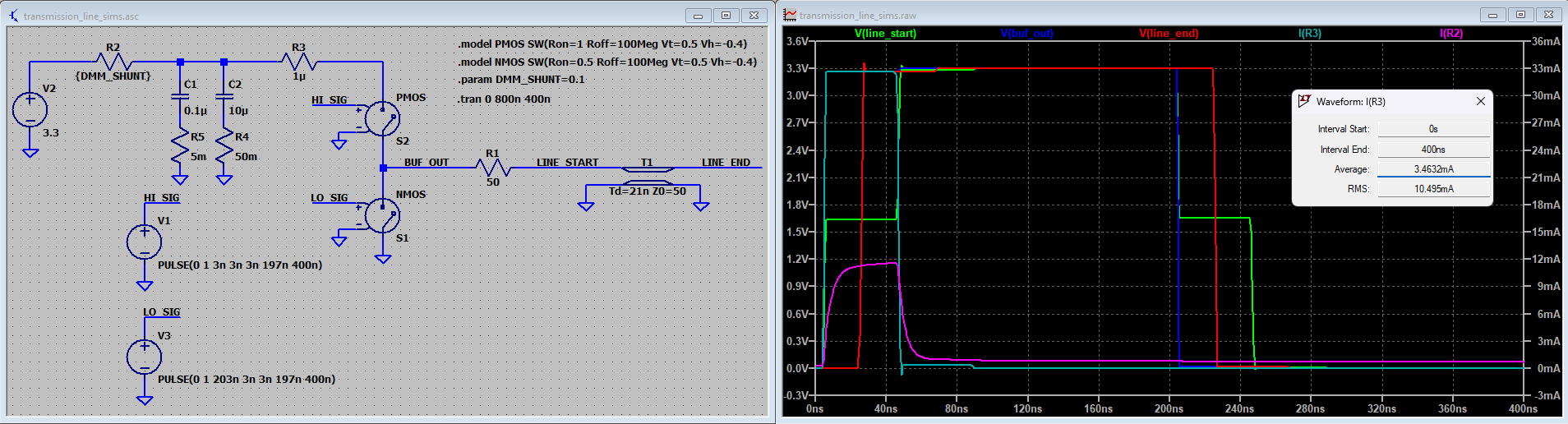
Screenshot of an LTSpice simulation showing a source-terminated transmission line case.
This may present something of a problem. Take an example of a garden-variety 74-series logic gate and see what it specs as the output drive capability at 3.3V.
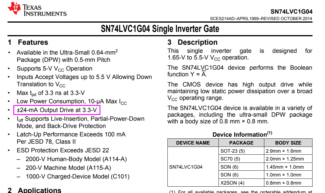
Snippet from the TI SN74LVC1G04 inverter datasheet.
Many logic gates will provide less than that. More on this matter at another time....
To Terminate or not to Terminate? Closing Remarks
As a closing remark, I wanted to address the subject of when it's necessary to add a discrete termination network. In my setup I had an unreasonably long transmission line (4.5m), whereas even the largest computer motherboard for example would be hard-pressed to have a trace longer than maybe 30cm. What's a good rule of thumb for when to terminate and when to not? And can we back it up with some non-hand-wavey reasoning? I will leave this topic for another post.
Author: Adam Cordingley
Date: 2024.2.10